
Main
Implantable bioelectronic devices can enable the continuous in situ monitoring and modulation of electrophysiological signals1,2,3,4. Traditional biomedical implants, such as pacemakers, neurostimulators and insulin pumps, typically rely on rigid and inorganic materials like silicon-based semiconductors, metals and oxides5,6. Though these have proven effective, their rigidity creates a large mechanical mismatch with soft biological tissues, which can result in complications such as microinjury, inflammation, fibrosis and necrosis over time7,8. To address these limitations, soft, lightweight and stretchable bioelectronic devices have been explored that could be seamlessly integrated with human tissues. These devices typically consist of two primary components: biointerface electrodes for signal acquisition and bioelectronic circuits for signal processing2,3,9,10,11. Despite advances in hydrogel-based electrodes, creating stretchable transistors for bioelectronic circuits that can offer high biocompatibility and stability in physiological environments remains a challenge12,13,14,15.
Stretchable organic electrochemical transistors (sOECTs) were initially proposed for skin-like electronic circuits due to their low Young’s modulus and compatibility with biological ionic media16. However, sOECTs have several drawbacks for electronic circuit applications, including high OFF currents and crosstalk due to their ion-based operation, which complicates the selection of individual devices in an array of transistors17,18,19. Furthermore, the high charging currents at the channel–electrolyte interface of sOECTs pose risks of undesired neural activation in vivo20. Stretchable organic field-effect transistors (sOFETs) are a promising alternative to sOECTs for high-frequency signal processing21. These devices leverage well-established field-effect transistor technologies and maintain mechanical flexibility and electrical performance, making them suitable for integration into bioelectronic circuits5,9,22,23,24,25,26,27,28,29,30.
Despite their potential, most sOFETs have been fabricated using industrial-grade elastomers, such as styrene–ethylene–butylene–styrene (SEBS), poly(styrene–butadiene–styrene), polyurethane and polydimethylsiloxane (PDMS), which are not certified for biocompatibility or may induce chronic foreign body reactions10. Medical-grade elastomers, particularly bromo isobutyl–isoprene rubber (BIIR), have been designed for biomedical applications and meet stringent biocompatibility standards set by health authorities, such as ISO 10993 and the European Pharmacopoeia31,32,33. BIIR exhibits excellent mechanical properties, including shock absorption, low permeability, aging resistance and high physical strength, alongside high chemical resistance and low reactivity with microorganisms34,35,36,37. These properties make it desirable for blending with semiconductors to create stable, biocompatible and stretchable transistors.
In this Article, we report the fabrication of skin-like implantable sOFETs using a vulcanized blend film of BIIR and poly[(dithiophene)-alt-(2,5-bis(2-octyldodecyl)-3,6-bis(thienyl)-diketopyrrolopyrrole)] (DPPT-TT) as the elastomer matrix and semiconductor, respectively. The resulting transistors exhibit stable electrical performance under mechanical strain, maintaining functionality even at 50% elongation. Furthermore, we integrate the dual-layer metallization of silver (Ag) and gold (Au) to create stretchable and biocompatible electrodes, ensuring robust performance in biofluid environments38. We perform in vitro and in vivo evaluations to confirm the biocompatibility and stability of our devices, which show no adverse effects on cell viability, proliferation or migration, as well as no major inflammatory response or tissue damage.
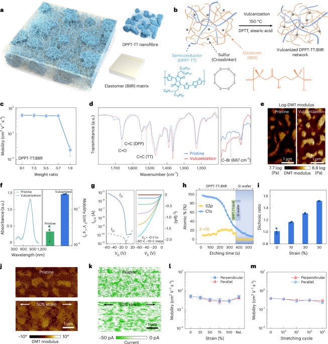
Material design and vulcanization of implantable semiconductors
Figure 1a presents the schematic of a biocompatible and stretchable semiconductor film comprising a semiconducting nanofibre network embedded within an elastomer matrix. The design uses a molecular blend of donor–acceptor-based semiconducting polymer with medical-grade rubber. We used DPPT-TT as the polymer semiconductor and BIIR as the biocompatible elastomer matrix. The blend film was chemically crosslinked through vulcanization, a well-established method to enhance the mechanical property of medical rubbers using additives such as sulfur (crosslinker), dipentamethylenethiuram tetrasulfide (DPTT; accelerator) and stearic acid (initiator; Fig. 1b). The phase separation that forms the semiconducting nanofibre network results from the surface energy disparity between DPPT-TT and BIIR, enabling the formation of a highly interconnected DPPT-TT nanofibre network within the elastic BIIR matrix, thereby imparting stretchability to the blend film (Supplementary Fig. 1 and Supplementary Note 1)28.

a,b, Schematic of the blend film (a) and vulcanization for implantable semiconductors (b). Chemical structures showing the semiconducting polymer (DPPT-TT), medical rubber (BIIR) and crosslinker (sulfur). c, Changes in mobility as a function of DPPT-TT:BIIR weight ratios (mean ± s.d.; n = 3). d, Fourier transform infrared spectra of the pristine and crosslinked blend films. e, DMT modulus mapping images of pristine (left) and crosslinked blend (right) films. f, Normalized UV–visible absorbance spectra (left) and mobility (right) of the pristine and crosslinked blend films (mean ± s.d.; n = 3). g, Transfer (left) and output (right) characteristics of the optimized blending weight ratio (3:7). D, drain; G, gate. h, XPS depth profiling of the blend film. i, Dichroic ratio of the blend film ranging from 0% to 50% uniaxial strain (mean ± s.d.; n = 3). j,k, AFM phase image (j) and C-AFM image (k) of the blend film with 0% and 50% strain. l, Mobilities of the blend film ranging from 0% to 50% uniaxially stretched and released states (mean ± s.d.; n = 3). Rel. indicates strain-released state. m, Mobilities of the blend film under multiple stretching cycles with 100% uniaxial strain.
To determine the optimal blend ratio for electrical and mechanical properties, we evaluated the vulcanized semiconductor films across various weight ratios of DPPT-TT and BIIR (1:9 to 9:1). The results showed stable field-effect mobility across the blend ratios, indicating that the semiconducting percolation path is preserved up to a 0.7 weight fraction of BIIR (Fig. 1c and Supplementary Fig. 2). This ratio produced a highly elastic semiconducting film that sustained up to 100% strain without mechanical damage, as confirmed by optical microscopy (OM) images of the 3:7 blend film (Supplementary Fig. 3). Conversely, the blend films with lower BIIR content (9:1 to 5:5) exhibited cracks at 25% strain, emphasizing the necessity of higher BIIR content for intrinsic stretchability. Therefore, the 3:7 blend ratio was optimized for the field-effect mobility, crack-onset strain and integrity of the semiconducting nanofibre network (Supplementary Figs. 4 and 5). The optimized composition ratio of the blend film achieved a balance between high elasticity and stable electrical performance, sustaining up to 100% strain without cracking and maintaining high field-effect mobility and its Derjaguin–Muller–Toporov (DMT) modulus, ranging from approximately 107.7 Pa to 108.8 Pa, aligns well with the mechanical properties of skin tissue, making it desirable for subcutaneous electronics1.
To verify the vulcanization of BIIR in the blend film, we performed Fourier transform infrared spectroscopy analysis (Fig. 1d and Supplementary Fig. 6). The vulcanization process involves three key reaction stages: initiation for radical formation, propagation for crosslinking BIIR with sulfur and termination for end of the reaction (Supplementary Note 2). The reduction in the C–Br (667 cm−1) peaks in the Fourier transform infrared spectra post-vulcanization confirmed the successful initiation (Fig. 1d). The reduction in the C=C peak (1,538 cm−1) in neat BIIR post-vulcanization indicates successful propagation39. The blend film has difficulty decoupling the C=C peak of BIIR because DPPT-TT has a similar C=C peak, whereas the C=C peak was reduced in the neat BIIR film. The unchanged C=C peak of the blend film after vulcanization indicates that the conjugated bond structure of DPPT-TT was preserved. The increased modulus observed in the DMT modulus mapping further confirmed vulcanization, enhancing the elasticity of the blend film and preserving its pristine nanomorphology (Fig. 1e). Additionally, the unchanged UV–visible absorption spectra before and after vulcanization indicate that the vulcanization process selectively crosslinks BIIR chains without disrupting the conjugated molecular structure of DPPT-TT (Fig. 1f and Supplementary Figs. 7 and 8). Transistors fabricated with vulcanized blend films exhibited higher field-effect mobility and ON/OFF ratio, suggesting that vulcanization also serves as a thermal annealing process, optimizing the morphology of the semiconducting polymer film and crosslinking the BIIR elastomer (Fig. 1g). We also performed X-ray photoelectron spectroscopy (XPS) depth profiling of the vulcanized blend film, which revealed a uniform distribution of S atoms from DPPT-TT nanofibres throughout the semiconductor film, facilitating effective charge injection and transport in both vertical and horizontal directions (Fig. 1h). The dichroic ratio of the vulcanized blend film as a function of applied strain (0%–50%) showed a linear increase, indicating the alignment of semiconducting nanofibres along the strain direction without mechanical cracking (Fig. 1i and Supplementary Fig. 9). Furthermore, atomic force microscopy (AFM) and conductive AFM (C-AFM) images showed a highly interconnected DPPT-TT nanofibre network aligned with the strain direction, providing a strain-insensitive conductive path (Fig. 1j,k). This morphology was reflected in the stable electrical performance of the organic field-effect transistors, with negligible changes in mobility under strains from 0% to 100% on a rigid substrate (Fig. 1l and Supplementary Figs. 10 and 11). Additionally, the mobility of the blend film remained consistent after 1,000 stretching cycles at 100% strain, demonstrating excellent mechanical durability (Fig. 1m and Supplementary Fig. 12). These results confirm that the vulcanized blend film is highly stretchable, with the nanostructure of DPPT-TT well preserved under mechanical deformation.
Skin-like implantable active-matrix transistor
To develop skin-like and biocompatible implantable transistors, we used dual-layer metallization using Ag and Au to create highly conductive, stretchable and biocompatible electrodes38,40,41,42. Ag was selected for its excellent electrical contact properties, whereas Au provided robust protection against biofluid-induced corrosion, thereby enhancing the durability of the electrodes (Fig. 2a and Supplementary Fig. 13). XPS depth profiling confirmed an intermixing region of carbon (C) and Ag atoms, which enhances both stretchability and adhesion (Fig. 2b). Initial resistance measurements demonstrated that the Ag–Au dual-layered electrode maintained low resistance after soaking in artificial sweat for 72 h, indicating their high corrosion resistance. Transistors fabricated with the dual-layered electrodes exhibited electrical performance comparable with those having Ag or Au electrodes, with the added benefit of enhanced durability in biofluid environments (Fig. 2c). The dual-layered electrode was stretchable up to 50% and maintained a resistance of 102 Ω after soaking in artificial sweat for 72 h, demonstrating its viability for highly conductive, stretchable and biocompatible electrodes in skin-like implantable transistors (Fig. 2d and Supplementary Figs. 14–16).

a, OM images (top) of the Ag, Au and Ag/Au electrodes on the blend film after soaking in PBS (72 h) and resistance change in the Ag/Au electrode on the blend film (bottom). b, XPS depth profiling of the Ag/Au electrode and blend film. c, Transfer characteristics of the transistors with various source/drain electrodes. S, source. d, Resistance of Ag, Au and Ag/Au electrodes ranging from 0% to 50% uniaxially stretched and released states before and after soaking in artificial sweat during 72 h. e, Transfer characteristics of a skin-like implantable transistor with different drain voltages. f, Mobilities and ON/OFF currents of skin-like implantable transistors range from 0% to 50% uniaxially stretched and released states. g, Skin-like implantable transistor’s mobility and ON/OFF currents under multiple stretching cycles with 50% uniaxial strain. h, Drain currents changed after soaking in deionized water, saline and PBS for 72 h. i, Photographs of a skin-like implantable active-matrix transistor array (left) attached to the skin and placed on a replica of a human brain (right) with its cross-sectional structure. j, Distribution of ON current (left) and ON/OFF ratio (right) of 25 devices in the skin-like implantable active-matrix transistor array. k, ON currents (top) and mobilities (bottom) of the skin-like implantable active-matrix transistor array under different uniaxial strains (mean ± s.d.; n = 3).
Figure 2e shows the typical transfer characteristics of a skin-like implantable transistor at various drain voltages, demonstrating its capability to operate under low-voltage conditions essential for safe in vivo applications (Supplementary Fig. 17). The transistors maintained stable electrical performance and mechanical durability, retaining their initial field-effect mobility and ON/OFF ratios up to 50% strain, even after 10,000 stretching cycles (Fig. 2f,g and Supplementary Figs. 18–21). The robustness to biofluids was validated by negligible changes in the drain current after 72 h of soaking in various artificial sweat solutions (Fig. 2h and Supplementary Fig. 22), highlighting the effectiveness of Ag–Au dual-layer metallization in creating resilient and reliable electrodes for stretchable transistors.
To validate the practical applicability of our devices in circuits, we fabricated a 5 × 5 active-matrix array of skin-like implantable transistors that enable seamless contact with curvilinear skin surfaces and a wrinkled brain replica (Fig. 2i). The array demonstrated uniform drain current, field-effect mobility and ON/OFF ratio across all the devices, confirming its high yield and suitability for bioelectronic applications (Fig. 2j and Supplementary Fig. 23). The field-effect mobility of the active-matrix array showed consistent performance, with minimal variation in ON current and mobility under different uniaxial strains (Fig. 2k and Supplementary Fig. 24).
In vitro biocompatibility tests for skin-like implantable transistors
In vitro biocompatibility tests were conducted using human dermal fibroblasts (hDFs) and macrophages (Mφ) to evaluate the safety and effectiveness of the materials used in the implantable semiconductor and transistor. The tests assessed the impact of each material (BIIR, SEBS, blend film and fully assembled transistor) on cell viability, migration and gene expression.
A schematic of the in vitro experiment is shown in Fig. 3a. To assess the effects on cell viability and function, each material was indirectly co-cultured with hDFs or macrophages using a transwell system. Live/dead assays and Cell Counting Kit-8 (CCK-8) assays were used to assess the cell viability. Fluorescence microscopy results from the live/dead assay showed green signals for live cells and red signals (with white arrows) for dead cells. Minimal red signals were observed across all material groups, confirming high cell viability (Fig. 3b). CCK-8 assay results further supported these findings, showing no notable differences in cell viability among the groups (Fig. 3c). These results indicate that all materials used in the implantable transistor exhibit excellent biocompatibility.

a, Schematic of the in vitro tests. b, Representative fluorescence images of live (green) and dead (red with white arrow) assay. Scale bar, 250 μm. c, Cell viability of each group confirmed with CCK-8 assay (n = 6 biological replicates, two-sided one-way analysis of variance (ANOVA) with post hoc Tukey’s correction for multiple comparisons). d, Representative wound closure assay images of control (Ctrl) and blend film groups. Scale bar, 200 μm. e, Quantification of the wounded area in each group after cell migration (n = 6 biological replicates, two-sided one-way ANOVA with post hoc Tukey’s correction for multiple comparisons). f, Proliferation, apoptosis and migration-related gene expression of hDFs in each group (n = 5 biological replicates, two-sided two-way ANOVA with post hoc Tukey’s correction for multiple comparisons). g, Relative gene expression of macrophage in each group (n = 5 for Cd86, Cd80 and Cxcl10; n = 6 for Nos2 and Stat1 biological replicates, two-sided two-way ANOVA with post hoc Tukey’s correction for multiple comparisons). h,i, Antibacterial test of each group using E. coli (h) and S. aureus (i; n = 5 biological replicates, two-sided one-way ANOVA with post hoc Tukey’s correction for multiple comparisons). j, Representative images of green fluorescence from E. coli and S. aureus with various materials. Scale bar, 10 μm. For the positive control, glass coverslips were coated with 0.1% gelatin to promote bacterial attachment and biofilm formation. Each biological replicate was performed in a separate well, seeded with independently prepared mammalian cells or inoculated with independently cultured bacterial suspensions. Data are presented as mean ± s.d.; NS, not significant.
The effect of each material on cell migration was investigated using an in vitro wound closure assay with hDFs. Similar wound closure rates across all groups indicated that the materials did not impair the migration properties of hDFs (Fig. 3d,e and Supplementary Fig. 25). Gene expression analysis using quantitative real-time polymerase chain reaction (qRT-PCR) revealed no major differences in the expression of proliferation-related protein encoded genes (PCNA and MKI67) and apoptosis-related protein encoded genes (BAX and BCL-2) among the groups, except for a substantial increase in the CXCR4 gene expression in the blend film group. This increase suggests the enhanced migration of hDFs in the presence of the blend film, which could contribute to the formation of a fibrous capsule (Fig. 3f). However, to evaluate the potential of each material to promote myofibroblast differentiation and enhance extracellular matrix synthesis, we examined the expression levels of genes encoding TGFβ1, COL1A1, COL2A1, COL3A1 and FN1, and found no important increase in the blend film group compared with control conditions (Supplementary Fig. 26).
The inflammatory potential was assessed by profiling gene expression in macrophages (RAW264.7 cells). After co-culturing macrophages with each material, the expression levels of specific markers associated with pro-inflammatory (M1) macrophages were measured. The BIIR induced the lowest expression level of Cd86-encoding gene, whereas other groups showed comparable expression levels (Fig. 3g). Both blend film and BIIR groups exhibited balanced profiles of genes encoding Cd80, Stat1 and Nos2 compared with the control. By contrast, the SEBS group exhibited the highest levels of gene expression, suggesting a higher propensity for inducing inflammation.
The antibacterial properties of the materials were evaluated using genetically modified strains of Escherichia coli and Staphylococcus aureus expressing the green fluorescent protein. The positive control group (gelatin-coated glass coverslip) showed notably higher bacterial growth, whereas the BIIR, SEBS, blend film and transistor groups exhibited no notable differences in bacterial numbers, indicating effective antibacterial properties (Fig. 3h,i). Representative fluorescence images confirmed lower bacterial viability on the blend film than bare PDMS (Fig. 3j). These results indicate an enhanced antibacterial effect of the fabricated DPPT-TT:BIIR, suggesting its potential application in medical devices.
Indirect co-culture in vitro tests demonstrated that the DPPT-TT:BIIR blend film and the fully assembled transistor exhibited high biocompatibility, supporting cell viability, proliferation and migration without inducing inflammatory responses. Nevertheless, it is essential to recognize that cellular responses in implanted environments can vary greatly depending on the mechanical and electrical properties of the substrates43,44. We characterized these substrate properties through surface energy, DMT modulus and C-AFM measurements, confirming the differences among the tested materials. (Supplementary Table 1 and Supplementary Fig. 27). Despite these differences, indirect culture methods inherently possess limitations in capturing subtle biological responses directly influenced by substrate stiffness, electrical conductivity and surface chemistry. To overcome these limitations, we conducted additional direct cell culture experiments in which exogenous electrical stimulation was applied to hDFs cultured directly on the blend film substrates. Under these conditions, large voltage- and duration-dependent changes were observed in cell viability and gene expression associated with fibrotic responses (Supplementary Fig. 28). This finding implies the importance of direct cell culture models as complementary methods capable of capturing nuanced biological interactions.
In vivo biocompatibility tests for skin-like implantable transistors
To evaluate the in vivo biocompatibility of the blend film, a comprehensive set of tests was conducted using a subcutaneous implant model in a BALB/C mouse (Fig. 4a). These tests aimed to assess the inflammatory response, tissue integration and overall compatibility of the materials over a prolonged period. Hierarchical clustering heat-map analysis revealed no major differences between the sham and implanted groups (Fig. 4b). Principal component analysis was performed on genetic data from each group, involving 19 genes listed in Table 1. Five principal components were identified, with PC1 accounting for 46.54% (eigenvalue, 8.843) and PC2 accounting for 35.06% (eigenvalue, 6.660) of the variance. Il10 and Nos2 (positive direction) and Il6 (negative direction) influenced PC1, whereas Il1β (positive direction) and Krt14 (negative direction) influenced PC2 (Fig. 4c). The distribution of principal component scores for the sham and implanted groups revealed no substantial differences, indicating compatibility of the materials with biological tissues and their suitability for long-term implantation (Fig. 4d).

a, Schematics of the in vivo test experiment. Scale bar, 5 mm. b, Hierarchical clustering heat map of the gene expressions in the sham and blend film groups. c, Distribution of the measured gene expression levels in the sham and blend film groups. d, Principal component analysis score based on the gene expression measurement in each group. e, Comparison of macrophage phenotype markers between the sham and blend film groups with a western blot analysis (n = 4 biological replicates, defined as individual mice treated independently; two-sided one-way ANOVA with Šídák’s test for multiple comparisons; mean ± s.d.). f, Immunohistochemistry of iNOS (green, left panel), CD163 (green, right panel) and CD68 (red) for pro- and anti-inflammatory macrophage staining. The lower side of the image is the implanted site. g, Comparison of fibrous capsule formation by H&E (top row), MT (middle row) and α-SMA (bottom row) staining. Top: H&E staining of the skin retrieved from the implanted site of each group. The black dashed line indicates the implanted site. Middle: MT staining result of the red dashed box in the H&E staining image (bidirectional arrows indicate the thickness of the fibrous capsule). Bottom: α-SMA immunofluorescence staining image of each group. dWAT, dermal white adipose tissue; PC, panniculus carnosus. Mouse icons in a created with BioRender.com.
Macrophage phenotyping confirmed the absence of major inflammatory responses. Western blot analysis demonstrated similar expression levels of M1 and M2 macrophage markers between the sham and implanted groups, indicating that no severe inflammation occurred—an essential factor for maintaining tissue homeostasis (Fig. 4e and Supplementary Fig. 29). This suggests that the materials integrate well with the host tissue, without causing adverse reactions. Immunohistochemistry for the M1 and M2 macrophage markers further supported these findings. Sections stained for iNOS (M1 marker), CD163 (M2 marker) and CD68 (Mφ marker) showed no notable differences between the sham and implanted groups, confirming that the blend film implantation did not provoke an inflammatory response (Fig. 4f). Next, we performed in vivo subcutaneous implantation for 30 days to observe fibrous capsules in the implanted site. To compare the extent of fibrous capsule formation on the blend film, we used PDMS and SEBS as comparison groups, as these materials are widely used for the encapsulation of implantable bioelectronics due to their high biocompatibility45,46,47,48. Before the in vivo experiment, we carried out migration experiments by indirect co-culturing with PDMS, SEBS and the blend film. In terms of in vitro migration, no differences were observed among PDMS, SEBS and the blend film (Supplementary Fig. 30). This result indicates that substances released from PDMS, SEBS and the blend film did not influence the cellular behaviour, accounting for the similar migration patterns observed. Following the 30-day-period in vivo experiment, all groups implanted with PDMS, SEBS and blend films exhibited the formation of fibrous capsules around the implantation site (Fig. 4g (top), blue dashed line) within the superficial fascia layer, as observed in the haematoxylin and eosin (H&E) staining. To assess the thickness of the fibrous capsules around the implantation site, Masson’s trichrome (MT) staining was performed. Although fibrous capsules formed around the implants in all three groups, the thickness of the fibrous capsules was observed to be lower in the SEBS and blend film groups compared with the PDMS group (Fig. 4g (middle), MT staining). A quantitative comparison of the thickness of the fibrous capsule also revealed that SEBS and blend films had a lower thickness compared with PDMS (Supplementary Fig. 31). Furthermore, the formation of fibrous capsules is known to be primarily driven by myofibroblasts49. Immunofluorescence staining for α-SMA, a marker of myofibroblasts, also showed that the formation of myofibroblasts around the implantation site was lower in SEBS and blend films compared with PDMS (Fig. 4g, bottom). On comprehensive analysis, we found that although the in vitro migration assays revealed similar cell migration behaviour across the PDMS, SEBS and blend film groups, actual fibrous capsule formation was the highest in PDMS implants in vivo. This discrepancy can be primarily attributed to the influence of mechanical properties, particularly the elastic modulus and stiffness, which greatly affect the fibrotic responses in vivo49. PDMS possesses a higher elastic modulus than SEBS, resulting in greater mechanical mismatch with the surrounding tissues, thereby facilitating myofibroblast activation and increased fibrous capsule thickness. However, indirect co-culture migration assays inherently focus on the cytotoxicity of the released soluble factors rather than capturing subtle mechanical influences. Consequently, these in vitro assays may not fully reflect the mechanical cues critical to fibrous capsule formation that are observed in vivo. Overall, the reduced fibrous capsule thickness observed around the blend film implants indicates improved mechanical compatibility with native tissues, potentially enhancing the long-term device functionality by minimizing fibrosis-related insulation issues.
Skin-like implantable circuits for bioelectronics
To demonstrate the practical applicability of skin-like transistors for implantable bioelectronics, we fabricated various logic circuits, including inverters, NOR gates and NAND gates (Supplementary Fig. 32). These circuits serve as fundamental components for constructing complex bioelectronic systems capable of advanced signal processing within the human body.
Figure 5a provides a schematic of the subcutaneous implantation of logic circuits fabricated with skin-like implantable transistors. These circuits were designed to maintain stable electrical performance under mechanical strain and physiological conditions. Pseudo-complementary-metal–oxide–semiconductor-based inverter, NOR and NAND devices are presented in Fig. 5b,f,h, respectively. The corresponding circuit diagrams and logic tables for each device are provided in Fig. 5c,g,i. To validate the functionality of our logic circuits in vivo, we implanted the devices into BALB/C mice and monitored their performance over 3 days. The inverter showed stable voltage transfer characteristics with apparent switching behaviour under 50% strain (Fig. 5d). The gain of the inverters remained consistent even after implantation and mechanical stretching, highlighting their robustness and stability under biological conditions (Fig. 5e). This stable performance is crucial for reliable signal processing in bioelectronic applications. The NOR and NAND gates maintained their logical output states under the same conditions, demonstrating robust performance despite mechanical deformation (Fig. 5j,k and Supplementary Figs. 33–36). The capability of these logic gates to function reliably under strain is critical for the development of flexible and dependable bioelectronic circuits. These results are comparable with state-of-the-art performance metrics of implantable transistors reported over the past five years (Supplementary Table 2).

a, Schematic of the in vivo subcutaneous implant model for testing function of the logic device. Scale bar, 5 mm. b, Photograph of an inverter device. c, Circuit diagram and logic table of the inverter. d,e, Voltage transfer characteristics (d) and gains of the inverter (e) at 0% strain (left) and 50% strain (right) before and after implanting into the mouse. f, Photograph of a NOR device. g, Circuit diagram and logic table of the NOR device. h, Photograph of a NAND device. i, Circuit diagram and logic table of the NAND device. j,k, Input (j) and output (k) characteristics of the binary logic device at 0% strain and 50% strain before and after implanting into the mouse. l, Comparison of macrophage phenotype markers between the sham and logic-device-implanted groups using western blot analysis (n = 4 biological replicates, defined as an individual mouse treated independently; two-sided one-way ANOVA with Šídák’s test for multiple comparisons; mean ± s.d.). m, Histology of the skin site with logic device implantation. Scale bar, 200 μm. Mouse icons in a created with BioRender.com.
The NAND and NOR gates retained stable electrical characteristics, including consistent output voltages, throughout the implantation period (Fig. 5k). The long-term stability in a physiological environment highlights the suitability of our devices for real-world bioelectronic applications. In vivo biocompatibility was assessed by analysing the inflammatory markers and histological features. Quantitative data and representative western blot images for M1 and M2 macrophage markers, as well as inflammation-related markers, are presented in Fig. 5l and Supplementary Fig. 37. All markers, except CD163, exhibited similar expression levels to those observed in the sham group, indicating that the implantation of the logic device did not induce severe inflammation. Additionally, short-term (3 days) implantation resulted in no detectable immune cell infiltration at the implantation site in either group (Fig. 5m). These findings demonstrate that our semiconductor-based elastomeric circuits are highly suitable for implantable electronics, exhibiting robust functionality and stability in biological environments. The sustained electrical performance observed after implantation underscores their potential for diverse biomedical applications, including real-time physiological signal monitoring, advanced neural interfacing and closed-loop therapeutic interventions. Moreover, their inherently soft, stretchable and skin-like mechanical properties facilitate seamless integration with dynamic biological tissues, minimizing mechanical-mismatch-induced stress and reducing the risk of chronic inflammation or fibrosis-related complications. Thus, our skin-like transistor technology represents a highly promising, versatile and clinically relevant platform that could accelerate the development of next-generation biomedical devices.
Conclusion
We have reported the development of sOFETs using a vulcanized blend film of a semiconducting polymer nanofibre and a biocompatible elastomer. The transistors exhibit high mechanical flexibility and can maintain stable electrical performance under up to 50% strain. Dual-layer metallization of Ag and Au for the electrodes ensures excellent electrical contact and resistance to biofluid-induced corrosion. Our in vitro biocompatibility assessments with hDFs and macrophages confirmed that the DPPT-TT blend does not negatively impact the cell viability, proliferation and migration or cause inflammation, as well as exhibits antibacterial properties. An in vivo study using a subcutaneous implant model in BALB/C mice demonstrated no major inflammatory response or severe fibrous capsule formation, confirming the suitability for long-term implantation. Furthermore, we fabricated skin-like implantable transistors and logic circuits, including active-matrix arrays, inverters, and NOR and NAND gates, and showed that they maintain functionality under mechanical stress and physiological conditions. This work addresses the critical challenges of mechanical mismatch and biocompatibility for implantable devices. These biocompatible sOFETs are suitable for several bioelectronic applications, offering a promising platform for medical devices that can seamlessly integrate with biological tissues. Future research will focus on optimizing the device performance and exploring applications in medical diagnostics and therapeutic interventions.
Methods
Materials
Au (99.99%, 3-mm granules) and Ag (99.99%, 3–5-mm granules) were purchased from SYSCIENCE. DPPT-TT was purchased from Derthon. BIIR (Mw = 684,730 g mol−1; Supplementary Fig. 38) was provided by Samsung Medical Rubber. SEBS H1062 and SEBS H1052 were provided by Asahi Kasei. H1062 (S/EB weight ratio, 18/82) and H1052 (S/EB weight ratio, 20/80) were used as the elastic substrate and dielectric layer, respectively. Anhydrous toluene (99.8%), anhydrous chlorobenzene (99.8%), anhydrous chloroform (99.8%), sulfur, DPTT, trichloro(octadecyl)silane and stearic acid were purchased from Sigma-Aldrich. PDMS (SYLGARD 184) and the curing agent were purchased from Dow Corning. PDMS was cured at a ratio of 11:1 (base/curing agent, w/w) at 55 °C overnight for the stamp. Silicon wafer (SiO2/Si, <100>, 1–30 Ω, 300-nm SiO2) was purchased from iTASCO. All the chemicals were used as received without further purification.
Device fabrication
Organic thin-film transistor on a rigid substrate
The solution for the semiconductor was prepared by dissolving 0.8 wt% of DPPT-TT, BIIR and crosslinker at various blending ratios in anhydrous chlorobenzene at 120 °C for 4 h. BIIR, sulfur, DPTT and stearic acid were added in a ratio of 100:1:1:5 and used as the elastic matrix of the semiconducting films. The solutions for the semiconductor were spun on an trichloro(octadecyl)silane-treated SiO2/Si wafer at 800 rpm for 1 min after filtration with a PTFE-D (0.2 μm) filter. The semiconducting film was annealed at 150 °C for 1 h. All processes were performed under a N2 atmosphere in a glovebox (H2O < 0.01 ppm and O2 < 0.01 ppm). The dielectric solution was prepared by dissolving 60 mg ml−1 of SEBS H1052 in toluene at 60 °C for 4 h. The dielectric solution was spun at 1,000 rpm for 1 min on an indium tin oxide (sheet resistance, 20 Ω sq−1) glass substrate. The semiconducting film was transferred from an trichloro(octadecyl)silane-treated wafer onto an SEBS/indium tin oxide glass substrate using PDMS stamps. The Ag source/drain electrodes were evaporated at 0.2 nm s−1 using a thermal evaporator. The channel length and width were 1,000 μm and 150 μm, respectively.
Fully stretchable transistors
The elastic substrates for the fully stretchable transistor were prepared by casting SEBS H1062 (100 mg ml−1 in toluene) onto glass slides. After drying overnight, the Au (30 nm)/Ag gate electrode (30 nm) was evaporated onto an SEBS substrate at 0.2 nm s−1 under a high vacuum (below 5.0 × 10⁻⁶ torr). The SEBS H1052 dielectric and semiconducting film (3:7 ratio of DPPT-TT to BIIR) were continuously transferred onto the gate electrode. Au/Ag source/drain electrodes (30 nm each) were evaporated onto the semiconducting films at a speed of 0.05 nm s−1. The channel length and width were 1,000 μm and 150 μm, respectively.
Fabrication of active-matrix transistor array
All procedures for the fabrication of the active-matrix transistor array were identical to those for the fabrication of fully stretchable transistors, except for the dielectric film, which was designed using a different concentration (75 mg ml−1 in toluene, spin coated at 1,000 rpm for 1 min) to obtain a thicker dielectric film (1.9 μm). The channel length and width were 2,000 μm and 150 μm, respectively.
Fabrication of logic gate devices including inverter, NAND and NOR
The SEBS substrate, semiconducting thin film and dielectric layer were prepared using the same process as that used for the fully stretchable active-matrix transistor array. The bottom Au (30 nm)/Ag electrodes (30 nm) were evaporated onto the SEBS H1062 substrates designed for each logic gate. The semiconducting films and dielectric layers were sequentially transferred onto the Ag electrode. Finally, the top Au (30 nm)/Ag electrodes (30 nm) were thermally evaporated using a designed pattern.
Stretchable and biocompatible encapsulation layer
The encapsulation films were prepared by casting the BIIR solution (120 mg ml−1 in chlorobenzene) on a Teflon mould, which was dried for 2 days and annealed at 150 °C for 30 min. The encapsulation films were applied to both sides (top and bottom) of the stretchable device.
Characterization
The devices were stabilized by aging them overnight in an autodry desiccator (24% humidity, 27 °C). The electrical characteristics of the devices were measured using a probe station connected to a Keithley 4200 device under atmospheric conditions, and a vacuum probe station with a Peltier device was connected to a Keithley 2636B device to control the temperature (Supplementary Note 3). The dielectric capacitance was measured using a probe station connected to an LCR meter (Keysight 4274A). UV–visible–near-infrared spectroscopy was performed using Jasco V-770. The surface structure was observed using AFM (Bruker MultiMode 8-HR) under ambient conditions. OM images were acquired using a Leica 2DM4 M device. The film thickness was measured using an ellipsometer (WONWOO STRC-2000). To obtain the stretched OM and AFM images, the semiconductor was transferred using the PDMS stamp method.
Cell culture
hDFs were purchased from Lonza. The hDFs were cultured in Dulbecco’s modified Eagle’s medium (Gibco BRL) supplemented with 10% (v/v) foetal bovine serum (Gibco BRL) and 1% (v/v) penicillin–streptomycin (Gibco BRL). The cells were incubated at 37 °C with 5% CO2 saturation. The cell culture medium was changed every 2 days. Cells within eight passages were used for the experiments. RAW264.7 cells were cultured in Dulbecco’s modified Eagle’s medium (Gibco BRL) supplemented with 10% (v/v) foetal bovine serum and 1% (v/v) penicillin–streptomycin.
Indirect co-culture with materials
hDFs or RAW264.7 cells were seeded in 6-well or 24-well cell culture plates (Corning) for all the experimental groups (control, BIIR, SEBS, blend film and logic device). One day after seeding, indirect co-culture with each material (225 mm2 for 6-well plates and 16 mm2 for 24-well plates) on a glass substrate was performed using 6-well and 24-well transwell inserts (8.0-µm pore size, Corning).
Fluorescein diacetate/ethidium bromide staining assay
Fluorescein diacetate (FDA; Sigma-Aldrich) and ethidium bromide (EB; Sigma-Aldrich) were used for FDA/EB staining. FDA (green) stains the cytoplasm of viable cells, whereas EB (red) stains the nuclei of non-viable cells. The staining solution was freshly prepared by combining 10 ml of FDA stock solution (1.5 mg ml−1 of FDA in dimethyl sulfoxide), 5 ml of EB stock solution (1 mg ml−1 of EB in phosphate-buffered saline (PBS)) and 3 ml of PBS. hDFs were then incubated in the staining solution for 3 min at 37 °C. After staining, the samples were washed twice with PBS and examined under a fluorescence microscope (DFC 3000G, Leica).
Cell viability
Cell proliferation was analysed using the CCK-8 (Sigma-Aldrich) assay. The hDFs were seeded in 24-well plates (2 × 10⁴ cells per well), and CCK-8 was used to measure the cell proliferation for 1 day after co-culturing with each material using a transwell system. The cells were washed in PBS, and the medium was replaced with a culture medium containing a CCK-8 solution (10%, v/v). After 2 h of incubation at 37 °C, the absorbance of each well was measured at 450 nm (Infinite F50, TECAN).
In vitro wound closure
The hDFs were grown in confluence in six-well plates50 and then replenished with Dulbecco’s modified Eagle’s medium (Gibco BRL). Thereafter, the cells were co-cultured sequentially using BIIR, SEBS, DPPT:TT:BIIR and logic devices for 1 day. A straight scratch was made on the hDF layer using a P1000 pipette tip. After incubation for 24 h, the gap width of the scratch following repopulation was measured and compared with the initial gap size at 0 h. The size of the denuded area was determined at each time point from the digital images using Adobe Photoshop CC.
qRT-PCR
The gene expression levels of human and mouse genes were quantified by performing qRT-PCR. Human-specific gene primers were utilized for the in vitro hDF analysis. Mouse gene primers were used for RAW264.7 cells and in vivo skin tissue analysis. The total ribonucleic acid was extracted from the samples using 1 ml of TRIzol reagent (Life Technologies) and 200 μl of chloroform. The lysed samples were centrifuged at 12,000g for 10 min at 4 °C. The ribonucleic acid pellet was then washed with 75% (v/v) ethanol in water and dried. Subsequently, the samples were dissolved in RNase-free water. For qRT-PCR, the SsoAdvanced Universal SYBR Green Supermix kit (Bio-Rad) and CFX Connect real-time polymerase chain reaction detection system (Bio-Rad) were used. Table 1 lists the primers used for qRT-PCR.
Antibacterial test
The antibacterial test was conducted using two representative bacterial strains commonly associated with infections on medical devices: E. coli and S. aureus. In this study, we used the genetically modified E. coli C2925 and S. aureus NCTC 8325-4 strains to express the green fluorescent protein. Both bacterial stains were cultured in a tryptic soy broth medium with ampicillin (100 μg ml−1) and chloramphenicol (10 μg ml−1) at 37 °C for 24 h, until an OD600 of 108 CFU ml−1 was reached in fresh media. Each strain was applied to a film sample (n = 6) prepared in a 24-well plate at a concentration of 5 × 10⁷ CFU ml−1 per well. For the positive control, gelatin (0.1% w/w)-coated glass coverslips promoting bacterial adhesion and growth served as positive controls along with bare PDMS blocks. In the experimental groups, the test films were placed in each well of a 24-well plate. After incubating at 37 °C for 24 h, non-adhered bacteria were removed by washing three times with PBS, and the bacterial colonies were fixed with a 4% paraformaldehyde solution for 10 min, followed by two washes with PBS. The bacteria were imaged using confocal microscopy (LSM800, Carl ZEISS) at ×40 magnification at the BT Research Facility Center, Chung-Ang University. The z-stacked images were processed using the maximum projection method, and the fluorescence intensity was measured using ImageJ (NIH) to quantify the relative number of bacteria adhered to each sample.
Exogenous direct current stimulation effect on hDF
hDFs were cultured directly on the blend film substrates deposited on Au electrodes and controlled exogenous electrical stimulation was applied. The surfaces were treated with oxygen plasma to enhance hydrophilicity, thereby promoting better cell adhesion. After seeding 2.5 × 10⁴ hDFs onto the blend films, we systematically investigated cell viability following d.c. electrical stimulation at varying voltages (0 mV, 100 mV, 200 mV, 300 mV and 500 mV) applied for 1 h (short term) and 24 h (long term). Cell viability was assessed by CCK-8 and gene expression of hDFs was assessed by qRT-PCR.
In vivo subcutaneous blend film and logic device implantation
Six-week-old female BALB/C mice (20–25-g body weight, Orient) were anaesthetized using 200 μl of xylazine (20 mg kg−1) and ketamine (100 mg kg−1) diluted in a normal saline solution. Hair was removed from the right side of the back using a combination of animal electric clippers and Nair (less than 1 min). The implanted site was marked with a 10 × 10 mm2 stamp on the lateral flank of each mouse. The epidermis, dermis and stratum corneum were surgically excised at the top and right sides. The skin was opened by flipping. For the blend film, SEBS, PDMS and logic device groups, each material was carefully implanted into the open area. An identical surgical procedure was performed for the sham group without implantation. After 3 days and 30 days, the subcutaneously implanted mice were killed for in vivo analysis. All animals were bred and maintained under specific pathogen-free conditions at the Laboratory Animals of Sungkyunkwan University and treated in accordance with institutional guidelines that were approved by the Institutional Animal Care and Use Committee of Sungkyunkwan University (SKKUIACUC2022-04-40-1 and SKKUIACUC2024-08-52-1).
Western blotting
The retrieved tissues were sectioned and lysed in RIPA buffer (Rockland Immunochemicals). After centrifugation at 10,000g for 10 min, the supernatant was prepared as a protein extract. Protein concentrations were determined using a bicinchoninic acid assay (Pierce Biotechnology). Equal amounts of protein from each sample were mixed with the sample buffer and subjected to sodium dodecyl sulfate–polyacrylamide gel electrophoresis using a 10% (v/v) resolving gel. The separated proteins were transferred to immune-blot polyvinylidene fluoride membranes (Bio-Rad). The membranes were blocked with 5% (w/v) skim milk in Tris-buffered saline (50 mM of Tris–HCl (pH 7.5) and 150 mM of NaCl, 2.5 mM of KCl), and incubated for 1 h at 25 °C. Then, the membranes were probed overnight at 4 °C with antibodies against glyceraldehyde 3-phosphate dehydrogenase (GAPDH; Abcam, ab9485), CD163 (Abcam, ab182422), CD206 (Abcam, ab64693), STAT1 (Cell Signaling Technology, CS9172), STAT6 (Cell Signaling Technology, CS9362) and TGF-β (Cell Signaling Technology, CS3711). Thereafter, the membranes were incubated in horseradish-peroxidase-conjugated secondary antibodies (R&D Systems, HAF008 for GAPDH, HAF017 for CD163, CD206, STAT1, STAT6 and TGF-β) for 1 h at 25 °C, followed by the addition of an enhanced chemiluminescence reagent (TransLab). The blots were developed in a dark room, and luminescence was recorded using an X-ray blue film (Agfa HealthCare).
Histology
Skin tissue specimens retrieved 3 days and 30 days post-implantation were fixed with a 4% paraformaldehyde solution and embedded using an optimum cutting temperature compound (SciGen Scientific). Thereafter, 10-μm sections obtained from the specimens were stained with H&E or MT stain to assess the fibrous capsule formation.
Immunohistochemistry
For immunohistochemical staining, the samples embedded in the optimum cutting temperature compound were cut into 10-μm-thick sections at −22 °C. To stain the pro-inflammatory macrophages, the sections were immunofluorescence stained with antibodies against INOS (Abcam, ab178945) and CD68 (Abcam, ab955). To stain the anti-inflammatory macrophages, the sections were immunofluorescence stained with antibodies against CD163 (Abcam, ab182422) and CD68 (Abcam, ab955). For observing the myofibroblast in a fibrous capsule, α-SMA (Abcam, ab5694) was used for immunofluorescence staining. INOS, CD163 and α-SMA signals were visualized using fluorescein-isothiocyanate-conjugated secondary antibodies (Jackson ImmunoResearch Laboratories). The CD68 signal was visualized using rhodamine (tetramethylrhodamine isothiocyanate)-AffiniPure goat anti-mouse IgG (Jackson ImmunoResearch Laboratories). The sections were counterstained with DAPI and examined via fluorescence microscopy (DFC3000 G, Leica).
Data availability
The data that support the findings of this study are available from the corresponding authors on request.
References
-
Sunwoo, S. H., Ha, K. H., Lee, S., Lu, N. & Kim, D. H. Wearable and implantable soft bioelectronics: device designs and material strategies. Annu. Rev. Chem. Biomol. Eng. 12, 359–391 (2021).
-
Song, Y., Min, J. & Gao, W. Wearable and implantable electronics: moving toward precision therapy. ACS Nano 13, 12280–12286 (2019).
-
Han, W. B., Ko, G. J., Jang, T. M. & Hwang, S. W. Materials, devices, and applications for wearable and implantable electronics. ACS Appl. Electron. Mater. 3, 485–503 (2021).
-
Mond, H. G. & Proclemer, A. The 11th world survey of cardiac pacing and implantable cardioverter‐defibrillators: calendar year 2009—a World Society of Arrhythmia’s project. Pacing Clin. Electrophysiol. 34, 1013–1027 (2011).
-
Yang, Y. et al. A non-printed integrated-circuit textile for wireless theranostics. Nat. Commun. 12, 4876 (2021).
-
Fang, H. et al. Capacitively coupled arrays of multiplexed flexible silicon transistors for long-term cardiac electrophysiology. Nat. Biomed. Eng. 1, 0038 (2017).
-
Discher, D. E., Janmey, P. & Wang, Y. L. Tissue cells feel and respond to the stiffness of their substrate. Science 310, 1139–1143 (2005).
-
Mazza, E. & Ehret, A. E. Mechanical biocompatibility of highly deformable biomedical materials. J. Mech. Behav. Biomed. Mater. 48, 100–124 (2015).
-
Wang, S. et al. Skin electronics from scalable fabrication of an intrinsically stretchable transistor array. Nature 555, 83–88 (2018).
-
Oh, J. Y. & Bao, Z. Second skin enabled by advanced electronics. Adv. Sci. 6, 1900186 (2019).
-
Hwang, S. et al. Integration of multiple electronic components on a microfibre towards an emerging electronic textile platform. Nat. Commun. 13, 3173 (2022).
-
Yang, Q. et al. Photocurable bioresorbable adhesives as functional interfaces between flexible bioelectronic devices and soft biological tissues. Nat. Mater. 20, 1559–1570 (2021).
-
Strakosas, X. et al. Metabolite-induced in vivo fabrication of substrate-free organic bioelectronics. Science 379, 795–802 (2023).
-
Xia, X. et al. Intrinsically electron conductive, antibacterial, and anti-swelling hydrogels as implantable sensors for bioelectronics. Adv. Funct. Mater. 32, 2206218 (2022).
-
Ren, H. et al. Injectable, self-healing hydrogel adhesives with firm tissue adhesion and on-demand biodegradation for sutureless wound closure. Sci. Adv. 9, eadh4327 (2023).
-
Li, N. et al. Bioadhesive polymer semiconductors and transistors for intimate biointerfaces. Science 381, 686–693 (2023).
-
Spyropoulos, G. D., Gelinas, J. N. & Khodagholy, D. Internal ion-gated organic electrochemical transistor: a building block for integrated bioelectronics. Sci. Adv. 5, eaau7378 (2019).
-
Cea, C. et al. Integrated internal ion-gated organic electrochemical transistors for stand-alone conformable bioelectronics. Nat. Mater. 22, 1227–1235 (2023).
-
Uguz, I. et al. Flexible switch matrix addressable electrode arrays with organic electrochemical transistor and pn diode technology. Nat. Commun. 15, 533 (2024).
-
Lee, W. et al. Integration of organic electrochemical and field-effect transistors for ultraflexible, high temporal resolution electrophysiology arrays. Adv. Mater. 28, 9722–9728 (2016).
-
Zhong, D. et al. High-speed and large-scale intrinsically stretchable integrated circuits. Nature 627, 313–320 (2024).
-
Dai, Y., Hu, H., Wang, M., Xu, J. & Wang, S. Stretchable transistors and functional circuits for human-integrated electronics. Nat. Electron. 4, 17–29 (2021).
-
Zhu, C. et al. Stretchable temperature-sensing circuits with strain suppression based on carbon nanotube transistors. Nat. Electron. 1, 183–190 (2018).
-
Nam, T. U. et al. Intrinsically stretchable floating gate memory transistors for data storage of electronic skin devices. ACS Nano 18, 14558–14568 (2024).
-
Nam, T. U. et al. Intrinsically stretchable phototransistors with polymer-QD-polymer multi-layered hybrid films for visible-NIR perspective electronic skin sensors. J. Chem. Eng. 492, 152143 (2024).
-
Kim, J. S. et al. Intrinsically stretchable subthreshold organic transistors for highly sensitive low-power skin-like active-matrix temperature sensors. Adv. Funct. Mater. 34, 2305252 (2024).
-
Oh, J. Y. et al. Intrinsically stretchable and healable semiconducting polymer for organic transistors. Nature 539, 411–415 (2016).
-
Xu, J. et al. Highly stretchable polymer semiconductor films through the nanoconfinement effect. Science 355, 59–64 (2017).
-
Vo, N. T. P. et al. Autonomous self-healing supramolecular polymer transistors for skin electronics. Nat. Commun. 15, 3433 (2024).
-
Choi, J. et al. Vertically stacked, low-voltage organic ternary logic circuits including nonvolatile floating-gate memory transistors. Nat. Commun. 13, 2305 (2022).
-
Ozdil, D. & Aydin, H. M. Polymers for medical and tissue engineering applications. J. Chem. Technol. Biotechnol. 89, 1793–1810 (2014).
-
Ohbi, D. S., Purewal, T. S., Shah, T. & Siores, E. Curing of bromobutyl elastomer composition using a xanthogen polysulphide accelerator for medical drug delivery device applications. J. Appl. Polym. Sci. 106, 526–533 (2007).
-
Ohbi, D. S., Purewal, T. S., Shah, T. & Siores, E. Crosslinking reaction mechanism of diisopropyl xanthogen polysulfide accelerator in bromobutyl elastomer for medical device applications. J. Appl. Polym. Sci. 107, 4013–4020 (2008).
-
Zhang, S. et al. Tacky elastomers to enable tear-resistant and autonomous self-healing semiconductor composites. Adv. Funct. Mater. 30, 2000663 (2020).
-
Cao, R. et al. Bromination modification of butyl rubber and its structure, properties, and application. Ind. Eng. Chem. Res. 58, 16645–16653 (2019).
-
Yang, S., Wu, H., Li, C., Xiong, Y. & Guo, S. Constructing oriented two-dimensional large-sized modified graphene oxide barrier walls in brominated butyl rubber to achieve excellent gas barrier properties. ACS Appl. Mater. Interfaces 12, 3976–3983 (2020).
-
Zhang, W. et al. Wearable and self-powered sensors made by triboelectric nanogenerators assembled from antibacterial bromobutyl rubber. Nano Energy 82, 105769 (2021).
-
Kim, M. H. et al. Mechanically robust stretchable semiconductor metallization for skin-inspired organic transistors. Sci. Adv. 8, eade2988 (2022).
-
Chumnum, K., Kalkornsurapranee, E., Johns, J., Sengloyluan, K. & Nakaramontri, Y. Combination of self-healing butyl rubber and natural rubber composites for improving the stability. Polymers 13, 443 (2021).
-
Chae, S. et al. Kinetically controlled metal-elastomer nanophases for environmentally resilient stretchable electronics. Nat. Commun. 15, 3071 (2024).
-
Sungwoo, S.-H. et al. Stretchable low-impedance conductor with Ag–Au–Pt core–shell–shell nanowires and in situ formed Pt nanoparticles for wearable and implantable device. ACS Nano 17, 7550–7561 (2023).
-
Sungwoo, S.-H. et al. Ventricular tachyarrhythmia treatment and prevention by subthreshold stimulation with stretchable epicardial multichannel electrode array. Sci. Adv. 9, eadf6856 (2023).
-
Kerr, C. M. et al. Decellularized heart extracellular matrix alleviates activation of hiPSC-derived cardiac fibroblasts. Bioact. Mater. 31, 463–474 (2024).
-
Kougkolos, G., Golzio, M., Laudebat, L., Nava, Z. V. & Flahaut, E. Hydrogels with electrically conductive nanomaterials for biomedical applications. J. Mater. Chem. B 11, 2036–2062 (2023).
-
Song, E., Li, J. & Rogers, J. A. Barrier materials for flexible bioelectronic implants with chronic stability—current approaches and future directions. APL Mater. 7, 050902 (2019).
-
Kim, S. et al. Wearable and implantable bioelectronics as eco‐friendly and patient‐friendly integrated nanoarchitectonics for next‐generation smart healthcare technology. EcoMat 5, e12356 (2023).
-
Wang, S. et al. Intrinsically stretchable electronics with ultrahigh deformability to monitor dynamically moving organs. Sci. Adv. 8, eabl5511 (2022).
-
Cheng, P. et al. An intrinsically stretchable power-source system for bioelectronics. Device 2, 100080 (2024).
-
Noskovicova, N. et al. Suppression of the fibrotic encapsulation of silicone implants by inhibiting the mechanical activation of pro-fibrotic TGF-β. Nat. Biomed. Eng. 5, 1437–1456 (2021).
-
Li, G. et al. Fabricating composite cell sheets for wound healing: cell sheets based on the communication between BMSCs and HFSCs facilitate full-thickness cutaneous wound healing. Tissue Eng. Regen. Med. 21, 421–435 (2024).
Acknowledgements
This research was supported by the Basic Science Research Program through the National Research Foundation of Korea (NRF) funded by the Ministry of Education (RS-2021-NR061555, RS-2020-NR049601), NRF funded by the Ministry of Science and ICT (MSIT) (RS-2024-00405818), GRRC program of Gyeonggi province (GRRCKYUNGHEE2023-B03) and the Korea Institute for the Advancement of Technology (KIAT) and the Ministry of Trade, Industry & Energy (MOTIE) of the Republic of Korea (RS-2024-00434908, RS-2021-KI002513 and RS-2025-25435993).
Ethics declarations
Competing interests
The authors declare no competing interests.
Peer review
Peer review information
Nature Electronics thanks Malavika Nair and Sung-Hyuk Sunwoo for their contribution to the peer review of this work.
Additional information
Publisher’s note Springer Nature remains neutral with regard to jurisdictional claims in published maps and institutional affiliations.
Supplementary information
Rights and permissions
Open Access This article is licensed under a Creative Commons Attribution-NonCommercial-NoDerivatives 4.0 International License, which permits any non-commercial use, sharing, distribution and reproduction in any medium or format, as long as you give appropriate credit to the original author(s) and the source, provide a link to the Creative Commons licence, and indicate if you modified the licensed material. You do not have permission under this licence to share adapted material derived from this article or parts of it. The images or other third party material in this article are included in the article’s Creative Commons licence, unless indicated otherwise in a credit line to the material. If material is not included in the article’s Creative Commons licence and your intended use is not permitted by statutory regulation or exceeds the permitted use, you will need to obtain permission directly from the copyright holder. To view a copy of this licence, visit http://creativecommons.org/licenses/by-nc-nd/4.0/.
About this article

Cite this article
Jung, K.H., Hyun, J., Jeong, M.W. et al. A biocompatible elastomeric organic transistor for implantable electronics. Nat Electron (2025). https://doi.org/10.1038/s41928-025-01444-9
-
Received:
-
Accepted:
-
Published:
-
DOI: https://doi.org/10.1038/s41928-025-01444-9